Skip to content
  • Career
  • Phone book
  • Events
  • MLZ Webpage
  • MLZ User Office
  • Webmail (internal)
  • Webmail ("Betrieb")
  • Intranet
  • de
  • en
  • Research Neutron Source Heinz Maier-Leibnitz (FRM II)
  • Technical University of Munich
Technical University of Munich
  • Home
  • About us
    • From "Atomic Egg" to FRM II
    • Facts & Figures
      • Auftragsvergaben
    • News & Media
      • News article
      • Films
        • Interactive panorama
      • Brochures
        • Annual Reports
        • Newsletter
      • Events
        • Maustag for Young and Old 2025
    • Contact
  • The Neutron Source
    • Neutrons
    • Fuel elements
      • Life cycle of a fuel element
      • Disposal of fuel elements
        • FRM II fuel element
        • Storage in Ahaus
        • Secure packaging
        • Transport vehicle
        • Permits
        • Function test
        • FAQ
      • Conversion
        • What does the conversion entail
        • Objectives of the conversion
        • Who is working on the conversion?
        • Fact check
    • Reactor
      • Installations in the pool
      • Guiding the beams
        • Cooling circuits
    • Irradiation facilities
      • Rabbit Irradiation
      • Capsule Irradiation
      • Mechanical Irradiation
      • Irradiation Position in the Control Rod
      • Irradiation with fast neutrons
      • Future Mo-99 irradiation facility
    • Safety
  • Safe all round
    • Protection of persons
    • Monitoring the facility
    • Monitoring the environment
      • Discharge of C-14
  • Transporte
  • Research
  • Medicine
    • Radioisotopes for diagnostics
    • Radioisotopes for therapy
    • Tumor irradiation
  • Industry
    • Materialanalyse
      • TUM-Expertenforen
      • VDI Fachausschuss 101
        • Bildgebende Verfahren
        • Optische Messverfahren
        • Eigenspannungs- und Texturanalyse
        • Analytik
      • Analysis with neutrons
    • Radioisotopes for industry
    • Silicon doping
  • Career
  • Guided Tours
  1. Home
  2. About us
  3. News & Media
  4. News article

Ultrafast quantum effects discovered in low-cost materials

Aktuell, Wissenschaft | 27.11.2025

A research team led by Professor Samuel Stranks at the University of Cambridge has observed ultrafast quantum phenomena in a simple, low-cost semiconductor material – a breakthrough that could make future quantum devices faster and more affordable. The necessary X-ray measurements were carried out by scientists from the Forschungszentrum Jülich at the Heinz Maier-Leibnitz Zentrum and at the Technical University of Munich.

Dr. Baohu Wu operates the small-angle scattering system KWS-X in the SAXS/WAXS Lab, JCNS at MLZ. © Bernhard Ludewig, FRM II / TUM

The research team has discovered that bulk formamidinium lead iodide (FAPbI₃) films produced using scalable solution or vapour deposition processes exhibit quantum emissions with extremely narrow line widths (less than 2 nanometres) and decay times in the picosecond range – light emissions that last only trillionths of a second. These effects arise naturally within nanodomain superlattices inside the material, without the need for expensive, precisely engineered structures.

Halide perovskites are promising materials for devices, such as solar cells, light-emitting diodes, and quantum light sources. However, achieving the ultrafast emission rates required for advanced quantum applications has typically been limited to more expensive materials.

Origin of quantum effects in the superlattice

Using ultrafast spectroscopy, cryogenic hyperspectral photoluminescence microscopy, and scanning electron diffraction, the researchers pinpointed the structural origin of these quantum effects: layered, nano-twinned superlattices formed by alternating corner-sharing and face-sharing octahedra. This periodic structure creates a natural, intrinsic quantum-confined environment.

The measurements were carried out at the SAXS/WAXS laboratory beamline at the MLZ in Garching. © Bernhard Ludewig, FRM II / TUM

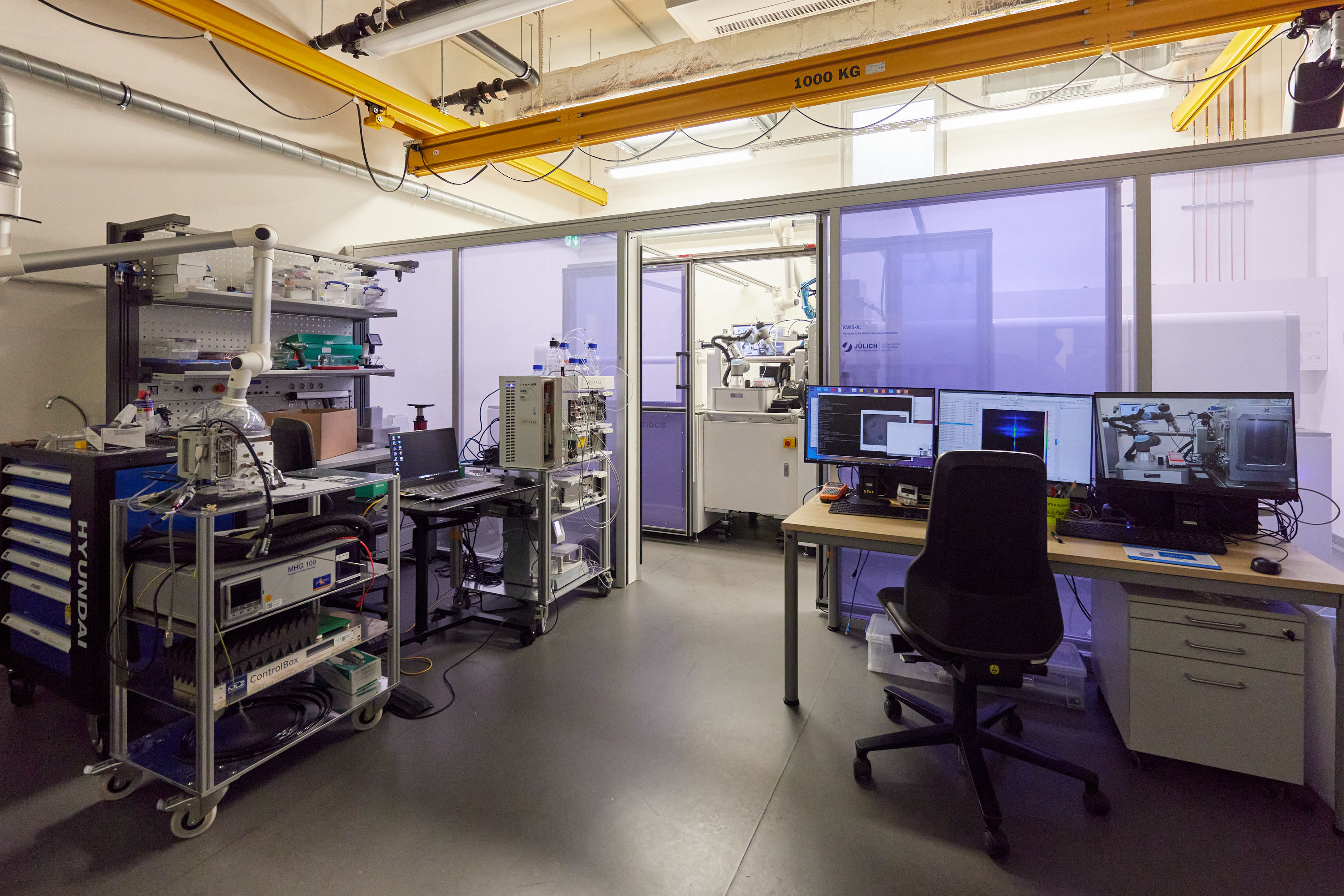
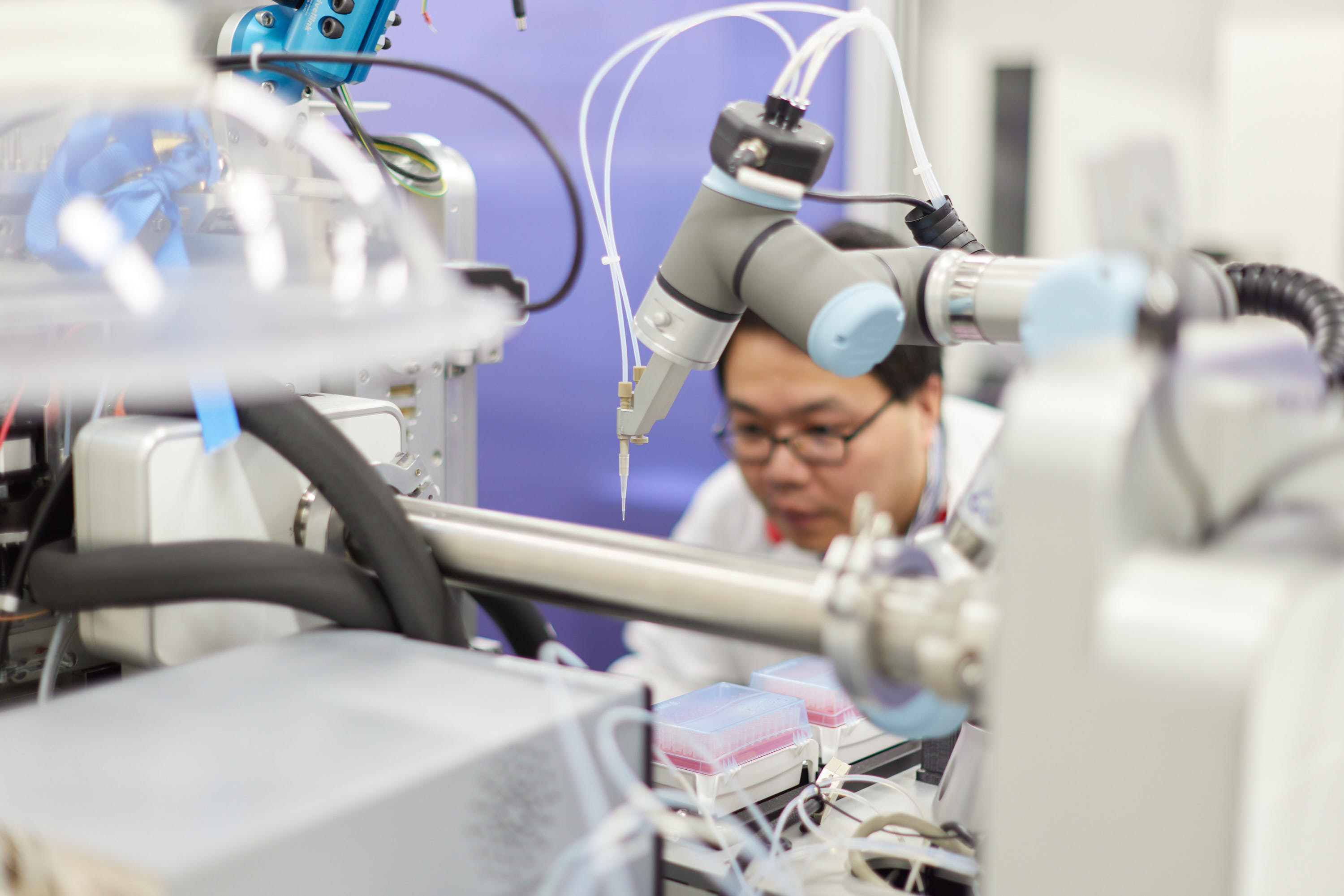
X-ray measurements at MLZ and TUM

The primary contribution to this research came from the team at the University of Cambridge, which managed the sample fabrication, ultrafast spectroscopic measurements, structural analysis, and data modelling. Cryogenic small- and wide-angle X-ray scattering (SAXS/WAXS) measurements, crucial for understanding the low-temperature structural behaviour, were provided by Dr. Baohu Wu at the Jülich Centre for Neutron Science (JCNS) at the Heinz Maier-Leibnitz Zentrum (MLZ) in Garching near Munich and Dr. Renjun Guo and Prof. Peter Müller-Buschbaum from the Department of Physics at the Technical University of Munich (TUM).

This discovery demonstrates that ultrafast quantum phenomena, previously only attainable in meticulously engineered materials, can be intrinsic to inexpensive, easily fabricated perovskite films. It opens up new pathways for designing high-performance quantum emitters for applications in ultrafast computing, communication, and sensing.

Original text: Angela Wenzik, Forschungszentrum Jülich.

Original publication: Dengyang Guo, Thomas A. Selby et al. “Picosecond quantum transients in halide perovskite nanodomain superlattices.” Nature Nanotechnology (2025). doi/10.1038/s41565-025-02036-6

Information on the SAXS/WAXS Laboratory Beamline of JCNS at the MLZ: The SAXS/WAXS Laboratory Beamline


Related News:

  • A protective layer for batteries - 19.05.2023
  • Skin-like Material Developed for Wearables - 13.09.2021
◄ Back to: News article
To top
  • Privacy
  • Imprint
  • Accessibility