Skip to content
  • Career
  • Phone book
  • Events
  • MLZ Webpage
  • MLZ User Office
  • Webmail (internal)
  • Webmail ("Betrieb")
  • Intranet
  • de
  • en
  • Research Neutron Source Heinz Maier-Leibnitz (FRM II)
  • Technical University of Munich
Technical University of Munich
  • Home
  • About us
    • From "Atomic Egg" to FRM II
    • Facts & Figures
      • Auftragsvergaben
    • News & Media
      • News article
      • Films
        • Interactive panorama
      • Brochures
        • Annual Reports
        • Newsletter
      • Events
        • Open day 2024
    • Contact
  • The Neutron Source
    • Neutrons
    • Fuel elements
      • Life cycle of a fuel element
      • Disposal of fuel elements
        • FRM II fuel element
        • Storage in Ahaus
        • Secure packaging
        • Transport vehicle
        • Permits
        • Function test
        • FAQ
      • Conversion
        • What does the conversion entail
        • Objectives of the conversion
        • Who is working on the conversion?
        • Fact check
    • Reactor
      • Installations in the pool
      • Guiding the beams
        • Cooling circuits
    • Irradiation facilities
      • Rabbit Irradiation
      • Capsule Irradiation
      • Mechanical Irradiation
      • Irradiation Position in the Control Rod
      • Irradiation with fast neutrons
      • Future Mo-99 irradiation facility
    • Safety
  • Safe all round
    • Protection of persons
    • Monitoring the facility
    • Monitoring the environment
      • Discharge of C-14
  • Research
  • Medicine
    • Radioisotopes for diagnostics
    • Radioisotopes for therapy
    • Tumor irradiation
  • Industry
    • Materialanalyse
      • TUM-Expertenforen
      • VDI Fachausschuss 101
        • Bildgebende Verfahren
        • Optische Messverfahren
        • Eigenspannungs- und Texturanalyse
        • Analytik
      • Analysis with neutrons
    • Radioisotopes for industry
    • Silicon doping
  • Career
  • Guided Tours
  1. Home
  2. Industry
  3. Silicon doping

Silicon Doping

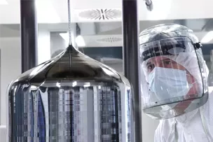
Silicon single crystal for the semiconductor industry.
© Siltronic

The silicon doping plant (SDA) is a purely commercial production facility at the FRM II. It is used for doping high-purity silicon, which is used in the semiconductor industry for high-performance electronics, for example. For example, they are used in thyristors that convert high currents from direct voltage to alternating voltage (thus enabling current transport over long distances) or power control in high-speed trains.

The FRM II can produce up to 15 tons per year, which is 10% of the global market.

Pure silicon is a very poor conductor of electricity. However, it becomes a technically usable semiconductor if it contains a small amount of foreign atoms (e.g. phosphorus). The introduction of these foreign atoms is called doping. At the research neutron source, doping is achieved with the help of neutrons: the silicon crystal is placed in the irradiation position and exposed to a precisely defined thermal neutron flux. The doping effect is based on the fact that the silicon isotope 30Si (around 3 % of naturally occurring silicon consists of this isotope) is activated during irradiation by capturing neutrons in a previously calculated manner and converted into stable 31P (phosphorus) with a half-life of 2.6 hours. In contrast to other doping techniques, the so-called neutron transmutation doping (NTD) described guarantees a particularly homogeneous P distribution in the silicon crystal.

The SDA at the FRM II can irradiate cylindrical Si single crystals with a height of up to 50 cm and a diameter of up to 20 cm. In order to achieve homogeneous doping, the neutron flux in the irradiation position of the SDA is smoothed by a suitable nickel coating and the irradiation basket also rotates around its own cylindrical axis during irradiation. The demand for silicon doped by neutron irradiation is so high that companies from Europe and Asia place orders for up to 15 tons per year at the FRM II. After irradiation, the silicon crystals have a specific resistance of 25 to 1000 Ωcm.

To top
  • Privacy
  • Imprint
  • Accessibility